Latest

We are pleased to announce that our distributor, Herzan LLC., will represent Spicer Consulting at ISTFA 2023. The ISTFA conference will be held on November 12-16th at Phoenix, Arizona. If you would like to learn how our Magnetic Field Cancelling System and SC28 Monitoring System may help improve the images of your electron microscopes, electron beam lithography systems, CD-SEMs, and focused ion beam tools, please stop by Booth #423. Contact Spicer Consulting Limited Contact Herzan LLC
The unparalleled magnification capabilities of electron microscopes (EMs) make them indispensable for applications requiring nanometre scale imaging. However, the sensitivity required to operate at such high magnification levels leaves them vulnerable to magnetic field perturbations, vibration and changes in temperature and humidity, all of which need to be kept to a minimum to ensure peak performance. Keeping track of such environmental factors is no mean feat, but dedicated continuous monitoring systems are now available to detect changes in instrument surroundings in real time, simplifying troubleshooting procedures and ensuring optimal device performance. Blurred lines The superior magnification offered by EMs stems from the use of electrons instead of light to probe a sample; the wavelength of these particles can be many orders of magnitude shorter than photons on the visible spectrum, enabling them to resolve much smaller features. The beam of electrons is focused on the specimen, and interacts with atoms in the sample to produce signals that contain information about surface topography and composition. Seeing details at such a small scale requires the beam to be perfectly positioned and focused, which can be compromised by external interferences from acoustic noise and vibrations, leading to blurred images. Additionally, since the electrons are charged particles, EM performance is also greatly affected by external magnetic fields. This leads to distinct artefacts appearing in the image; AC fields often show up as sharp jagged edges, while DC fields create wavy lines. EM manufacturers therefore precisely map and specify the degree of interference that their instruments can handle before the image quality drops below the acceptable limit.
Electron microscopes (EMs) are vital quality control (QC) tools in semiconductor production, helping manufacturers to guarantee a high standard of product. However, the precision of EMs and the resolution of resulting images can be hindered by external interruptions, such as acoustic noises, vibrations and magnetic fields. Low resolution and perturbed images can make it hard to detect faults in semiconductor products, which could in turn decrease the yield and performance of manufactured goods. Therefore, continually assessing the quality of the imaging environment and pinpointing any potential sources of disturbances is critical to maintaining a high standard of production. Fortunately, there are dedicated systems on the market designed especially for continuous monitoring of the environment surrounding sensitive EMs, which now provide uninterrupted and automatic logging of various environmental parameters to revolutionise electron beam (EB) instrument applications. Failure analysis is an important component of QC in semiconductor production, which can ultimately help to enhance yield and guarantee a high standard of manufacturing excellence. However, smaller and smaller semiconductor devices are being developed, making it increasingly difficult to perform failure analysis and locate defects in products. Various high-resolution EM tools – including scanning electron microscopy (SEM), focused ion beam scanning electron microscopy (FIB-SEM) and transmission electron microscopy (TEM) – are helping to analyse the structure of even the smallest devices. This is crucial for localising and characterising defects and electrical problems that may affect performance, solidifying these EM instruments as cornerstones of the QC process. Unfortunately, the environment in which the EM is located can have a significant impact on image quality, as external factors – such as acoustic noises, vibrations, and magnetic fields – lower the resolution and make it harder to find defects. In addition, these disturbances can also cause instability or shifts in the EB, resulting in significant reductions in resolution, so that instruments perform below their intended design specifications. It is therefore important to the quality of imaging that these types of disturbances are identified when the instrument is first installed within a semiconductor manufacturing or research environment. They must also be continually monitored throughout their use, as subsequent or transient changes to conditions can cause ongoing problems for operators. Surveying the environment Surveillance of the environment prior to installation should be a standard when investing in any EB instrument, in order to ensure that the microscope or lithography machine is placed in an appropriate location that will enable it to operate to its desired specifications. There are purpose-made survey systems for this application – such as Spicer Consulting's SC11 family – which are able to measure both vibrations and external magnetic fields. Once installed, many EB instrument users also perform long-term surveillance of the environment to help identify any drifts in continuous fields or transient disruptions that could impact performance. However, until recently, the technologies available for this ongoing environmental monitoring have been missing one critical feature – the ability to measure several parameters simultaneously without any interruptions in data collection. Continuous feedback An innovative monitoring system (SC28 Monitoring System, Spicer Consulting) that continuously logs magnetic fields and floor vibration in three axes, as well as acoustic levels, temperature and humidity, has recently launched onto the market. This system can be controlled via a computer connected to the same local area network, and all the gathered information is automatically stored in date-stamped files by the software. This program can also be used to define environmental specifications, either as minimum/maximum values, or as a spectrum of maximum amplitude versus frequency. The software constantly compares the measured values for each parameter with the user-defined specifications, and real-time results are displayed in a small window. The SC28 can be configured to send an email to the user if any parameters shift beyond the allowed margins. This can be done either once or at a specified frequency, making sure that the issue is dealt with in a timely manner. In addition, a traffic light beacon can be used to give a visual warning, something that can be useful in a manufacturing environment such as semiconductor production.

Spicer Consulting donated new Microsoft tablets to Clophill St Mary's Lower School and Nursery, and pay for the setting up and installation. We are thrilled that the tablets will be used by the children to complete their computing work. See details: https://www.facebook.com/clophillstmarysschool/posts/pfbid02tojRSLop1oFZfNz8d6HTwJQvYCgF7TVRXG9dmEpqS6gHc5ivX9C5P6gjThhyfEddl
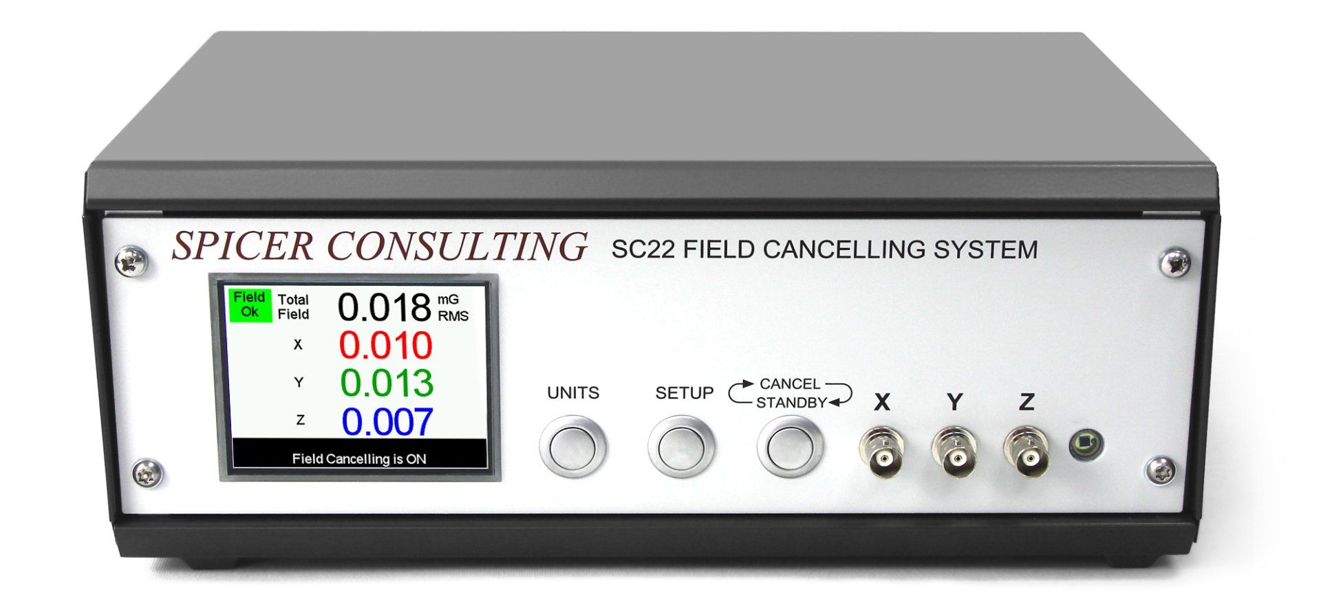
Magnetic fields are everywhere, radiating from such diverse sources as power networks, electrical equipment and even the earth’s core. For the most part, they do not interfere with everyday activities, but state-of-the art technologies operating at extreme levels of precision can be susceptible to even the most minute disturbances. For example, the image resolution of scanning electron microscopes (SEMs) can be negatively affected by magnetic field interference, preventing the equipment from being used to its full potential. Fortunately, magnetic field cancelling systems can attenuate such disturbances, and the University of Granada in Spain has recently installed an SC24 Magnetic Field Cancelling System to enhance the performance of its SEM set-up. Electron microscopes are used across a wide range of scientific disciplines, imaging everything from the inner workings of human cells to the complex crystalline structures of engineering materials, making access to state-of-the-art microscopy equipment essential for both academic and private researchers. Rocío Márquez Crespo, a technician at the University of Granada's Scientific Instrumentation Centre, explained: “I’m responsible for the Scanning Electron Microscopy Unit – located in the Faculty of Pharmacy – which provides services to research groups both here at the university and to other academic centres across Spain, as well as for many public institutions and private companies. As you can imagine, the applications we support are incredibly diverse, but the common thread running between them is the requirement for extremely high resolution images, and we accomplish this by providing access to both field emission and dual beam SEMs.” SEMs are well-known for their ability to measure features at the atomic level, but their precision and repeatability are heavily dependent on their surroundings, with factors such as vibration, temperature and humidity all affecting image quality. They are especially susceptible to external magnetic fields, since the images are generated using a beam of charged particles, which can be easily deflected by magnetic field disturbances. Rocío continued: “During the installation of our dual beam microscope, we noticed that images at the highest magnification settings were becoming distorted, and we suspected that it was due to magnetic field interference. An environmental survey carried out by the microscope manufacturer confirmed this to be true, and we were encouraged to purchase a magnetic field cancelling system to negate these effects. We’ve been recommended Spicer Consulting products many times in the past by colleagues and local researchers who’ve had positive experiences with them, so the SC24 Magnetic Field Cancelling System was the obvious choice.” The SC24 system comprises a magnetic field control unit, up to two magnetic field sensors, and three orthogonal axis multicore cables installed in the room where field cancellation is required. It stabilises the ambient field by dynamically creating nearly equal and opposite field changes, improving microscope performance. “Once the system was installed by Eloïse SAS – a local supplier – the high magnification image distortion disappeared at the flick of a switch. It was that simple,” Rocío concluded. Contact us f or more S C24 information. About Spicer Consulting Limited Spicer Consulting magnetic field cancelling systems protect electron beam instruments, including SEMs, transmission electron microscopes, electron beam lithography tools and SEM-based metrology and inspection tools. They are located in some of the world's leading laboratories, universities, semiconductor manufacturing plants and test facilities of electron and ion beam equipment manufacturers. The company’s magnetic field, vibration and acoustic analysis systems have also been adopted as the standard for conducting site surveys by leading equipment manufacturers. Spicer Consulting is located in Stewartby, Bedfordshire, within the United Kingdom’s golden triangle of elite universities in London, Cambridge and Oxford. About Eloïse SAS Eloïse SAS is a leading French scientific equipment company with 20 years of expertise in distributing and servicing electron microscopes and accessories. It offers the full Ted Pella/Pelco portfolio to French speaking countries, along with: vibrational & magnetic active compensation solutions (Spicer Consulting with K&S advanced); metallization and carbon evaporation equipment for sample preparation (Cressington); CCD-CMOS cameras for both on side and on axis TEM (Emsis); and nm resolution µ-electronic diffraction units for TEM, featuring 4D STEM with precession (NanoMEGAS). For more information, demos and training, visit Eloïse SAS at its Tremblay CDG AppLab, or explore the website at www.eloise-sarl.fr .
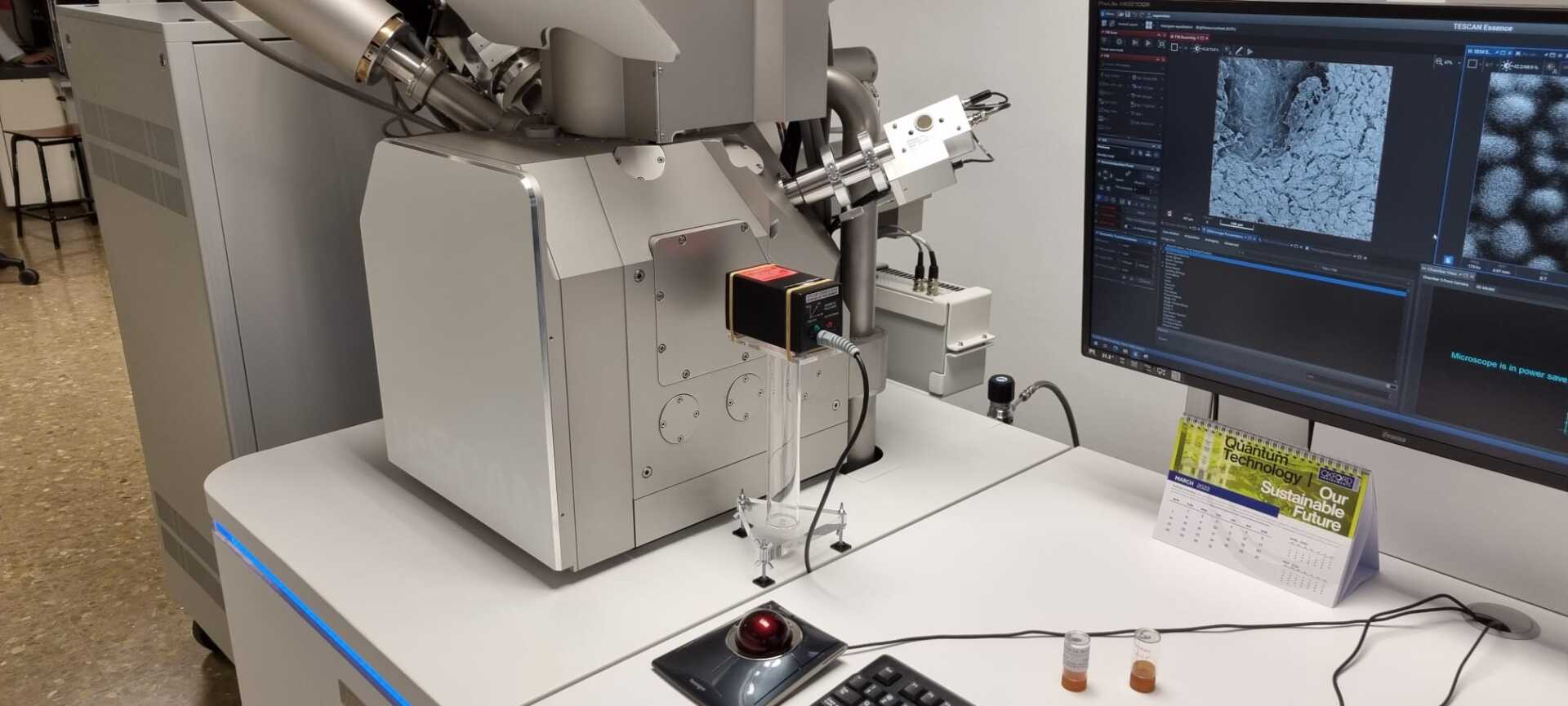
A company using Spicer Consulting's SC22 magnetic field cancelling system to improve the resolution of their SEM electron microscope.
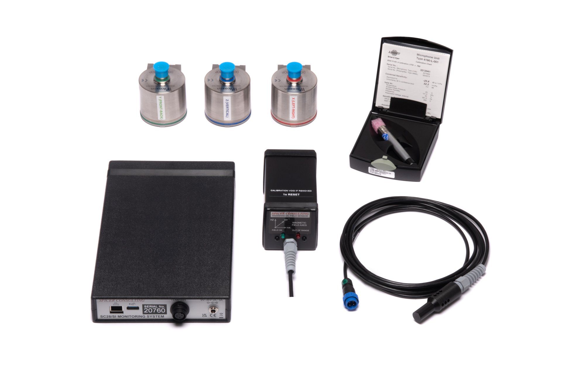
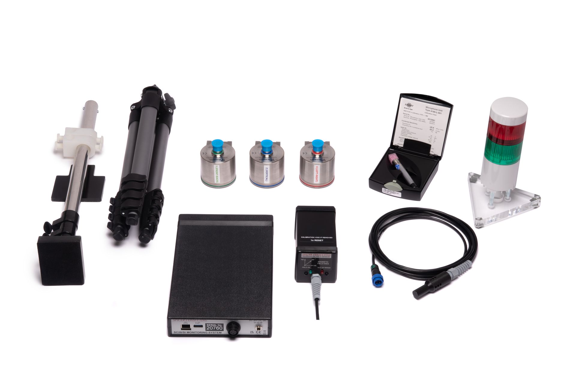
The SC11 Analysis System is for making surveys and the SC28 Monitoring System is for long term monitoring of the environment of electron microscopes and related tools. They use some of the same sensors, but for different purposes. The SC11 has higher performance, flexibility and automation for making surveys and troubleshooting at different sites. Our new SC28 is designed for continuous long term monitoring. It is suitable to be placed in one location and let it continuously log timestamped charts and spectra while also alerting you when the environment is out of specification. This provides electron microscope operators with complete peace of mind for the long-term stability of their instrumentation. Click here to see more comparisons between SC11 and SC28.
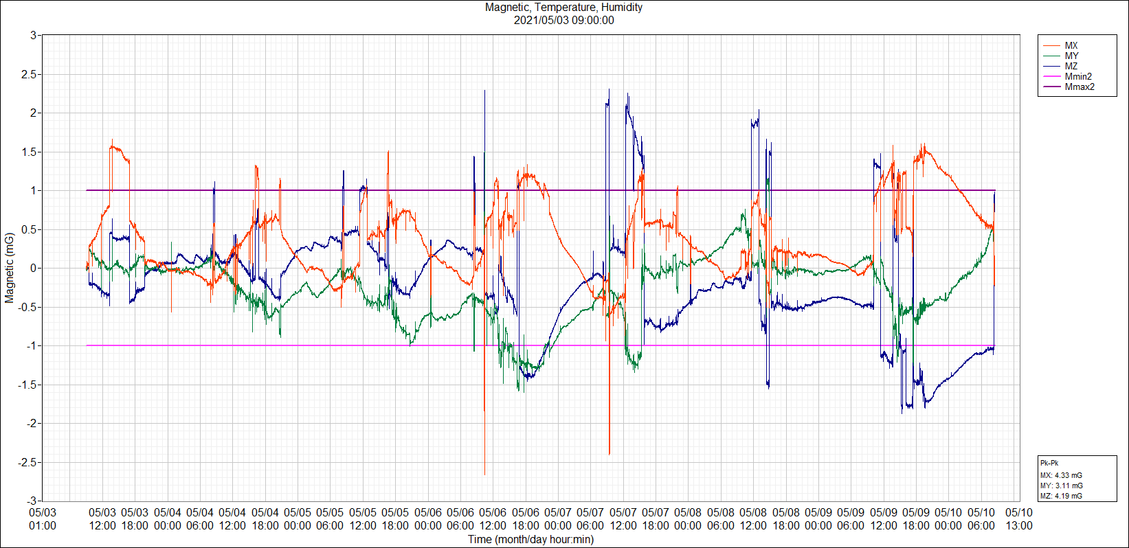
Spicer Consulting Limited is excited to introduce our new SC28 monitoring system. The SC28 enables long-term, uninterrupted monitoring of magnetic fields, vibrations and acoustics – as well as temperature and humidity – within the lab and semiconductor fab. This system is purposed-designed to monitor the environment for electron beam instruments, including Scanning Electron Microscopes (SEM), Transmission Electron Microscopes (TEM), Electron Beam Lithography tools and SEM-based metrology and inspection tools. Detecting stray magnetic fields, vibrations and other disturbances in the lab is very important for electron microscope applications since these can all negatively affect image quality and resolution. Based on customer feedback – especially from the semiconductor industry – Spicer Consulting Limited has developed the SC28 monitoring system to provide continuous measurements of the magnetic fields and vibrations in all three axes, as well as acoustics, temperature and humidity. The system’s software automatically records the live data and saves it to date-stamped files, making long-term monitoring of the lab seamless and easy. It can also be used as an alarm system to flag any issues, constantly comparing the measured environmental readings to the microscope specifications or user-determined thresholds, sending an error report if a parameter is out of specification. This provides EM operators with complete peace of mind for the long-term stability of their instrumentation. SC28 Product link www.spicerconsulting.com/sc28-monitoring-system
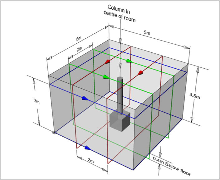
The production of semiconductor components on a nanometre scale has become more practical than ever, thanks to advancements in manufacturing. Electron microscopy – such as TEM, SEM and FIB-SEM – is an important quality control tool in the manufacture of these semiconductors, allowing structural analysis of devices to detect any problems. However, the image quality of these instruments is commonly affected by interference from surrounding magnetic fields, making it more challenging to identify manufacturing errors. The benefits of smaller components The semiconductor industry is under constant pressure to make components smaller. The desire to continually increase computing speed and power – while saving costs – means that more transistors are needed within each chip. However, placing additional transistors on a chip produces more heat. One way to keep the transistors cooler is to make them smaller, as the distance that the electrons have to move to do the same job is smaller, and therefore takes less energy. This also makes the whole system faster, which is more economical, as there is more functionality built into the same space on a silicon wafer. External factors can limit resolution Despite the advantages of creating smaller components, miniaturisation poses a challenge during manufacture, as a higher level of magnification is needed to inspect the parts. Electron microscopy is often used to perform due to the high resolution that this technique provides. When imaging features on a chip with an electron microscope, the electron beam must be positioned with a level of accuracy that is similar to the size of feature being examined to achieve required resolution. Unfortunately, electron microscopes are particularly sensitive to magnetic fields, which can deflect the electron beam. The smaller the object, and therefore higher the necessary resolution, the more sensitive the technique is to the surrounding magnetic fields – as well as vibrations and sound. The manufacturing environment will often experience a lot of magnetic field interference, as the most problematic frequency – around 60 Hz – is produced by an abundance of different machinery. As the space within most manufacturing sites is valuable, this leads to as many instruments as possible being packed into a given area, and this close proximity results in microscopy interference. In addition, newer semiconductor factories often feature ceiling-level monorail systems to transport components between stations for automatic loading and processing, which also helps with traceability of materials. These overhead systems typically create a 9 kHz magnetic field, which is incredibly detrimental to image quality and must be cancelled in order to improve resolution. Other contributing sources of magnetic field interference within semiconductor factories include magnetic stirrers used in plasma etchers and voice-coil actuated stages in lithography machines. Finding the most stable environment In the semiconductor industry, manufacturers often have highly-sensitive electron microscopes working alongside large pieces of industrial equipment – which produce various types of radiation – so it’s important to find a way to allow them both to work in harmony. This level of sensitivity requires areas to be surveyed meticulously before microscope installation, to ensure that the image quality produced will be unaffected by any external factors. Instruments such as Spicer Consulting’s purpose-designed SC11 Analysis System are routinely used by microscope vendors and consultants to perform site surveys for SEMs, TEMs and similar equipment. These instruments measure and analyse magnetic fields, vibrations and acoustics in X, Y and Z directions, displaying results graphically and allowing the user to perform a direct comparison between the fields encountered and the microscope specifications. This information is invaluable to ensure that electron microscopes are installed in the most stable environment possible – whether that is in an existing facility or a new laboratory – ensuring the highest possible image quality. Improving image resolution Top-end microscopes can only withstand minimal interference, so finding a suitable environment for the equipment can be extremely challenging. It is becoming increasingly common for electron microscope users to seek expert advice to find solutions to mitigate unwanted interferences, such as installing a magnetic field cancelling system. Spicer’s proprietary field cancelling technology has been developed over many years, and there are now thousands of these systems in use worldwide. All Spicer cancelling systems – including the popular SC24 – consist of a Magnetic Field Control Unit and one or more Magnetic Field Sensors, as well as three multicore cables, which are installed around the electron microscope. There are two different types of sensors that can be used depending on the interference present; the first only measures AC fields, whereas the other more complicated and high performance sensor can detect both high frequency AC and low frequency fields down to DC. The control unit includes power amplifiers that drive currents through the cables when interference is present, creating a nearly equal and opposite field. This dynamic response – which automatically compensates for field changes within 100 μs – stabilises the ambient field, restoring resolution. Conclusion There are many technical challenges involved in miniaturisation of semiconductor components, and both surveying instruments and cancelling equipment are essential in supporting the advancements within this industry. With a broad install base around the world, Spicer Consulting’s solutions have proven to be highly effective in restoring resolution in electron microscopes in manufacturing environments. For more information on how Spicer can help you optimise your EM, contact us to find out here . About Spicer Consulting Limited Since it was established in 1988, Spicer Consulting has built a world-wide reputation in magnetic field cancelling for Electron Microscopes and similar instruments. Today, working with equipment manufacturers and users alike, the company is recognised as an industry expert in maximising the performance of electron microscopes, electron beam lithography systems, CD metrology and focused ion beam tools. Spicer Consulting magnetic field cancelling systems protect sensitive equipment in the world's leading laboratories, universities and semiconductor manufacturing plants, as well as in the test facilities of electron and ion beam equipment manufacturers. Its magnetic field, vibration and acoustic analysis systems have been adopted as standard equipment for the conduct of site surveys by leading equipment manufacturers. Spicer Consulting is located in Stewartby, Bedfordshire, within the United Kingdom’s Golden Triangle of elite universities in London, Cambridge and Oxford.