Supporting miniaturisation in the semiconductor manufacturing industry
The production of semiconductor components on a nanometre scale has become more practical than ever, thanks to advancements in manufacturing. Electron microscopy – such as TEM, SEM and FIB-SEM – is an important quality control tool in the manufacture of these semiconductors, allowing structural analysis of devices to detect any problems. However, the image quality of these instruments is commonly affected by interference from surrounding magnetic fields, making it more challenging to identify manufacturing errors.
The benefits of smaller components
The semiconductor industry is under constant pressure to make components smaller. The desire to continually increase computing speed and power – while saving costs – means that more transistors are needed within each chip. However, placing additional transistors on a chip produces more heat. One way to keep the transistors cooler is to make them smaller, as the distance that the electrons have to move to do the same job is smaller, and therefore takes less energy. This also makes the whole system faster, which is more economical, as there is more functionality built into the same space on a silicon wafer.
External factors can limit resolution
Despite the advantages of creating smaller components, miniaturisation poses a challenge during manufacture, as a higher level of magnification is needed to inspect the parts. Electron microscopy is often used to perform due to the high resolution that this technique provides. When imaging features on a chip with an electron microscope, the electron beam must be positioned with a level of accuracy that is similar to the size of feature being examined to achieve required resolution. Unfortunately, electron microscopes are particularly sensitive to magnetic fields, which can deflect the electron beam. The smaller the object, and therefore higher the necessary resolution, the more sensitive the technique is to the surrounding magnetic fields – as well as vibrations and sound.
The manufacturing environment will often experience a lot of magnetic field interference, as the most problematic frequency – around 60 Hz – is produced by an abundance of different machinery. As the space within most manufacturing sites is valuable, this leads to as many instruments as possible being packed into a given area, and this close proximity results in microscopy interference. In addition, newer semiconductor factories often feature ceiling-level monorail systems to transport components between stations for automatic loading and processing, which also helps with traceability of materials. These overhead systems typically create a 9 kHz magnetic field, which is incredibly detrimental to image quality and must be cancelled in order to improve resolution. Other contributing sources of magnetic field interference within semiconductor factories include magnetic stirrers used in plasma etchers and voice-coil actuated stages in lithography machines.
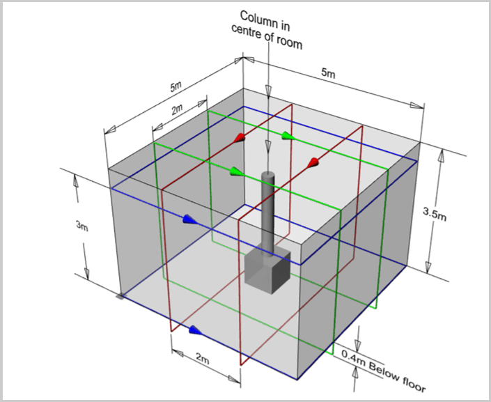
Finding the most stable environment
In the semiconductor industry, manufacturers often have highly-sensitive electron microscopes working alongside large pieces of industrial equipment – which produce various types of radiation – so it’s important to find a way to allow them both to work in harmony. This level of sensitivity requires areas to be surveyed meticulously before microscope installation, to ensure that the image quality produced will be unaffected by any external factors. Instruments such as Spicer Consulting’s purpose-designed SC11 Analysis System are routinely used by microscope vendors and consultants to perform site surveys for SEMs, TEMs and similar equipment. These instruments measure and analyse magnetic fields, vibrations and acoustics in X, Y and Z directions, displaying results graphically and allowing the user to perform a direct comparison between the fields encountered and the microscope specifications. This information is invaluable to ensure that electron microscopes are installed in the most stable environment possible – whether that is in an existing facility or a new laboratory – ensuring the highest possible image quality.
Improving image resolution
Top-end microscopes can only withstand minimal interference, so finding a suitable environment for the equipment can be extremely challenging. It is becoming increasingly common for electron microscope users to seek expert advice to find solutions to mitigate unwanted interferences, such as installing a magnetic field cancelling system. Spicer’s proprietary field cancelling technology has been developed over many years, and there are now thousands of these systems in use worldwide. All Spicer cancelling systems – including the popular SC24 – consist of a Magnetic Field Control Unit and one or more Magnetic Field Sensors, as well as three multicore cables, which are installed around the electron microscope. There are two different types of sensors that can be used depending on the interference present; the first only measures AC fields, whereas the other more complicated and high performance sensor can detect both high frequency AC and low frequency fields down to DC. The control unit includes power amplifiers that drive currents through the cables when interference is present, creating a nearly equal and opposite field. This dynamic response – which automatically compensates for field changes within 100 μs – stabilises the ambient field, restoring resolution.
Conclusion
There are many technical challenges involved in miniaturisation of semiconductor components, and both surveying instruments and cancelling equipment are essential in supporting the advancements within this industry. With a broad install base around the world, Spicer Consulting’s solutions have proven to be highly effective in restoring resolution in electron microscopes in manufacturing environments.
For more information on how Spicer can help you optimise your EM, contact us to find out here .
About Spicer Consulting Limited